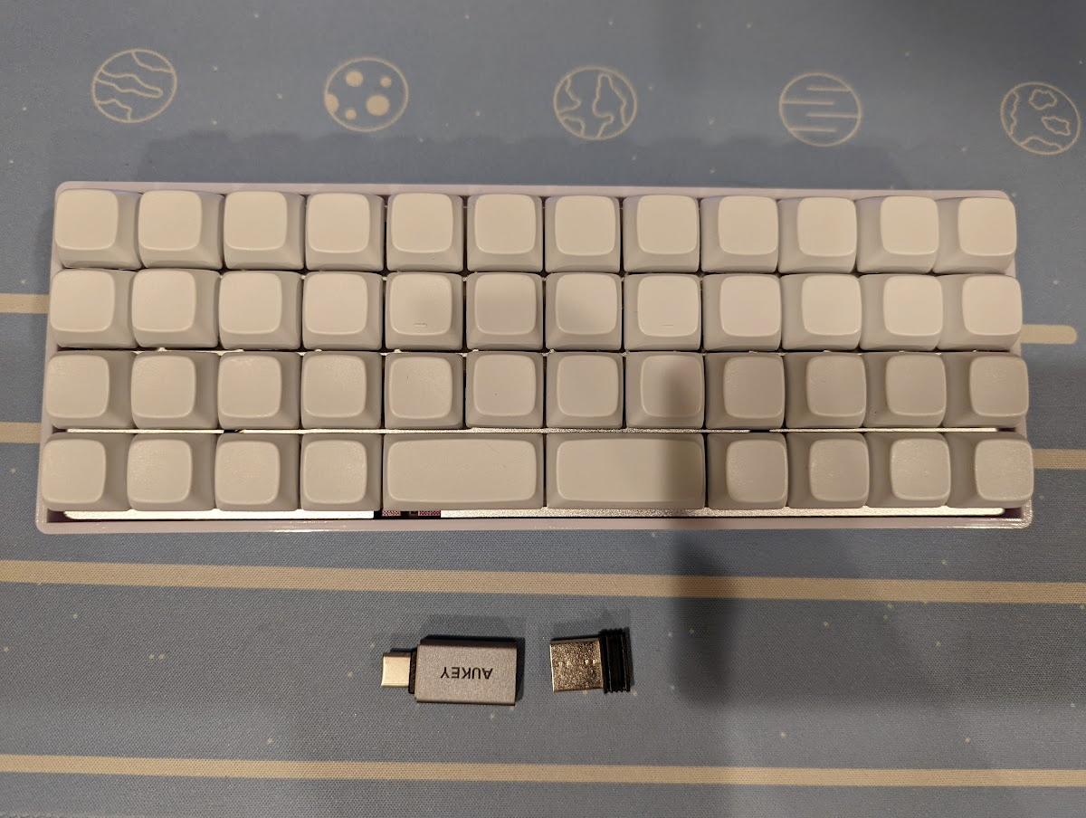
2.4 GHz Bluetooth USB dongles never seem to be USB-C. I find this dearth a bit annoying, because my MacBook Pro features only USB-C ports, and it seems silly that I’d have to carry around an awkward USB to USB-C port, if I ever wanted to use a Bluetooth dongle with my MacBook.
Fortunately, the popular YouTube channel, DIY Perks, noticed the same issue, and made a whole video about converting USB devices to USB-C:
I thought this tutorial would be perfect for my TU40 v3 keyboard, which has a 2.4 GHz Bluetooth dongle that connects via USB 2.0. In this post, I describe how I convert my keyboard’s Bluetooth dongle to USB-C, based on the DIY Perks video, above.
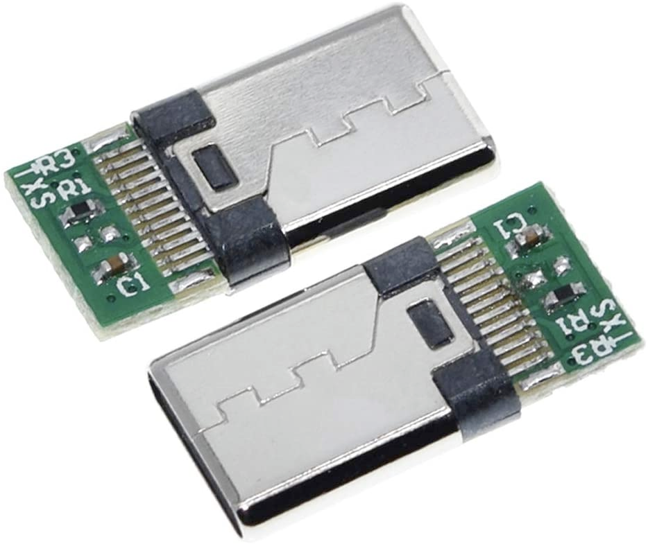
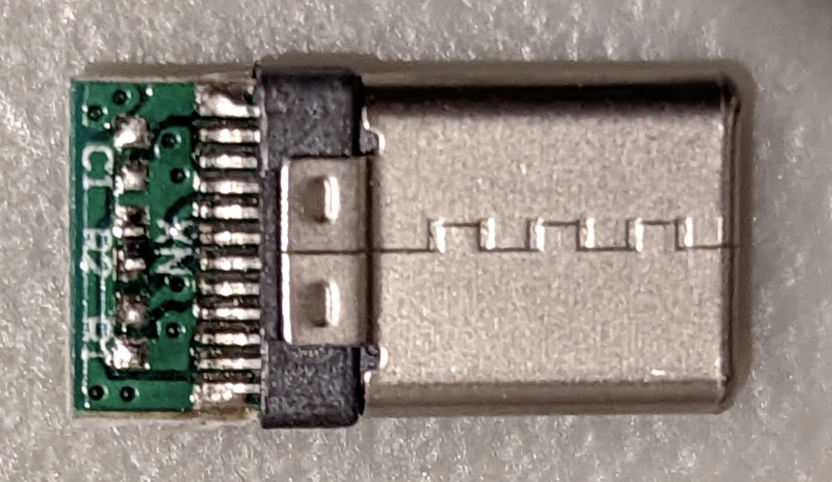
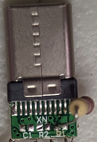
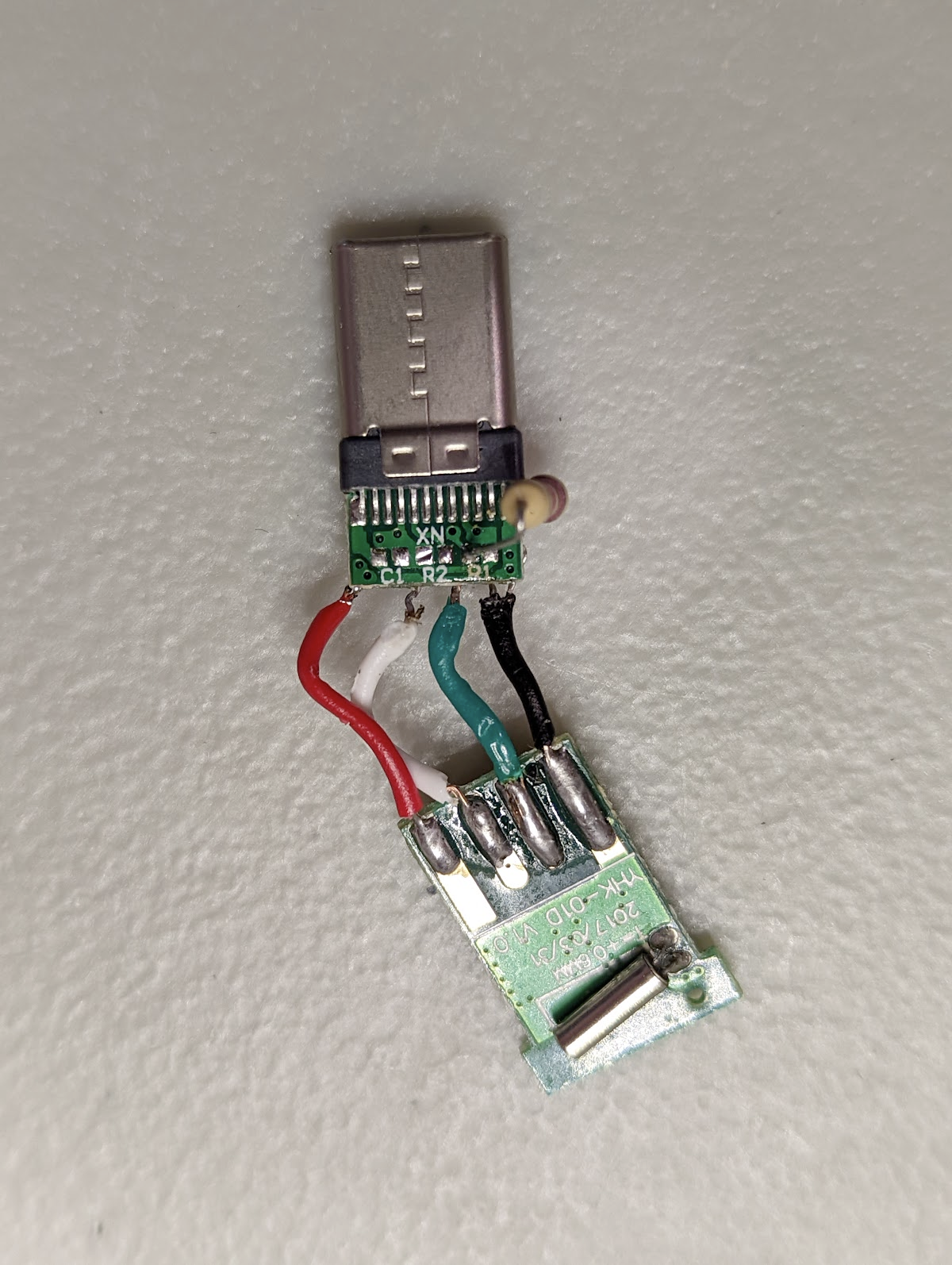
As is usually the case with these kinds of projects, I wasn’t able to get the exact USB-C breakout board that DIY Perks recommends, so I had to make some slight hardware adjustments, based on what’s available to me. First, I bought the male USB-C breakout board off Amazon (ASIN: B09WCQKSW1). The PCB I bought doesn’t have all the USB-C pins broken out. Rather, it just has the four main pins typical of USB 2.0 cables, broken out: V, D+, D-, and GND. By convention, V is red, GND is black, D+ is green, and D- is white. This USB-C breakout board, like almost all USB-C breakout boards, is configured as a host device. Even though I shouldn’t have felt surprised by this revelation, I was a little miffed because the Amazon photos for the product clearly show the PCB hardware-configured not as a host device:
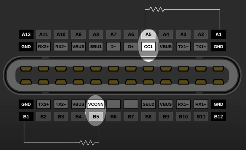
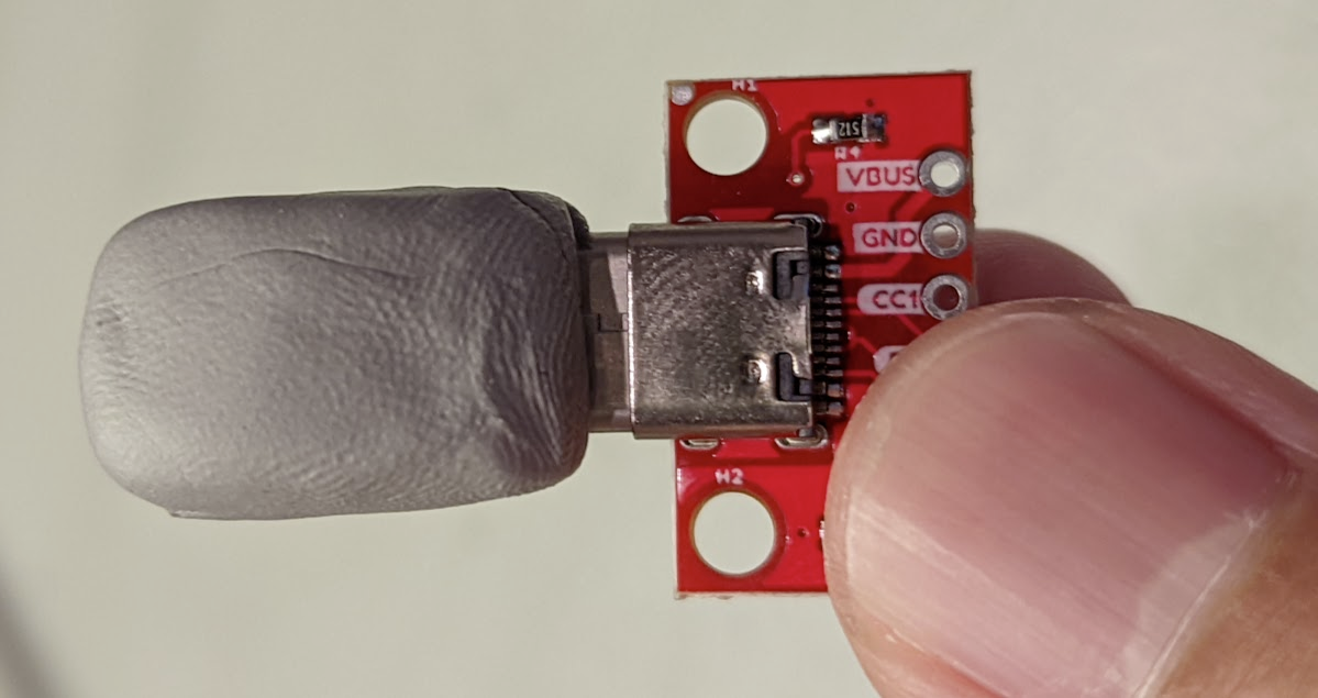
We want to configure the board as a sub-device, however, because we wish to use it as a receiver for a mechanical keyboard. To do so, we have to alter the host device configuration, which is defined by the implementation of pull-up resistor, to a sub-device configuration, which is defined by the implementation of a pull-down resistor. To see how we do this, let’s examine the pinout of USB-C:
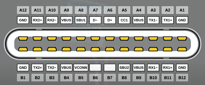
Like I mentioned already, a pull-up configuration configures the USB-C connection as a host device. In other words, a USB-C connection as a host device has the following:
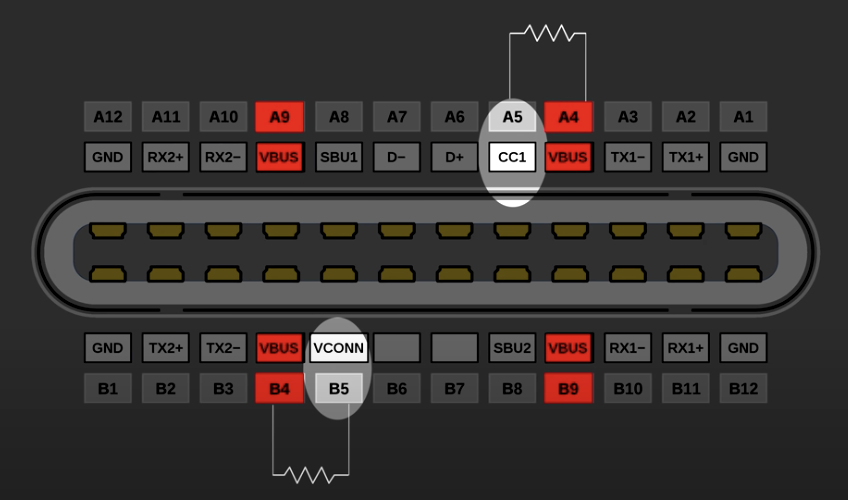
If we examine our PCB closely, the CC1 pin is indeed pulled up:
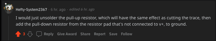
So we need to remove the resistor, R2, that is responsible for the pull-up and the host device configuration. In the DIY Perks video, Matt scrapes off a trace that goes from the pull-up resistor. I found this method to be pretty obnoxious, and Reddit actually suggested that it’d be better for me to completely desolder the pull-up resistor on R2:
Desoldering the resistor was easy enough!
We must now implement the pull-down resistor onto the CC1 pin:
To do so, I solder in a 4.7 kOhm resistor from GND to the CC1 pin, like they do in the video.
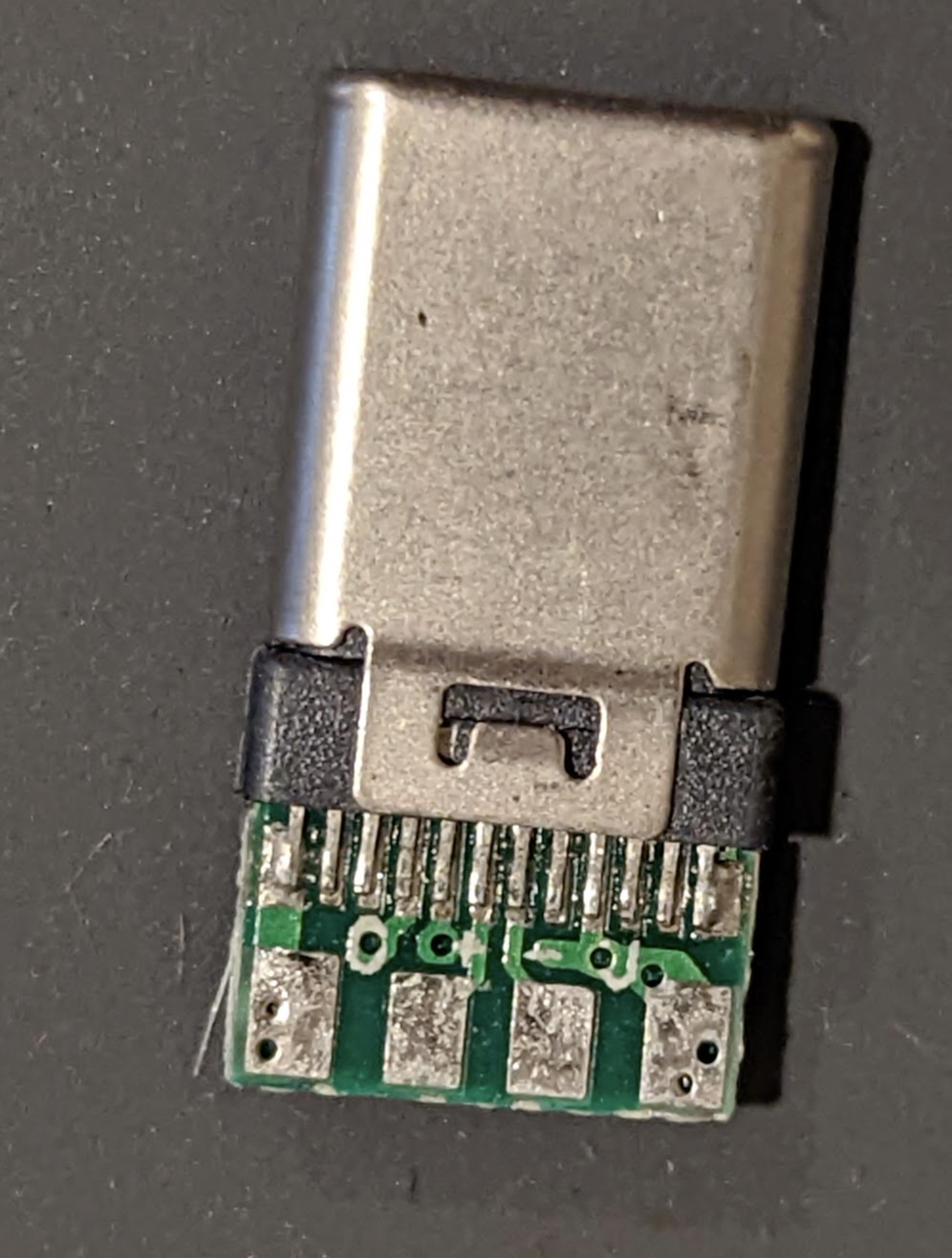
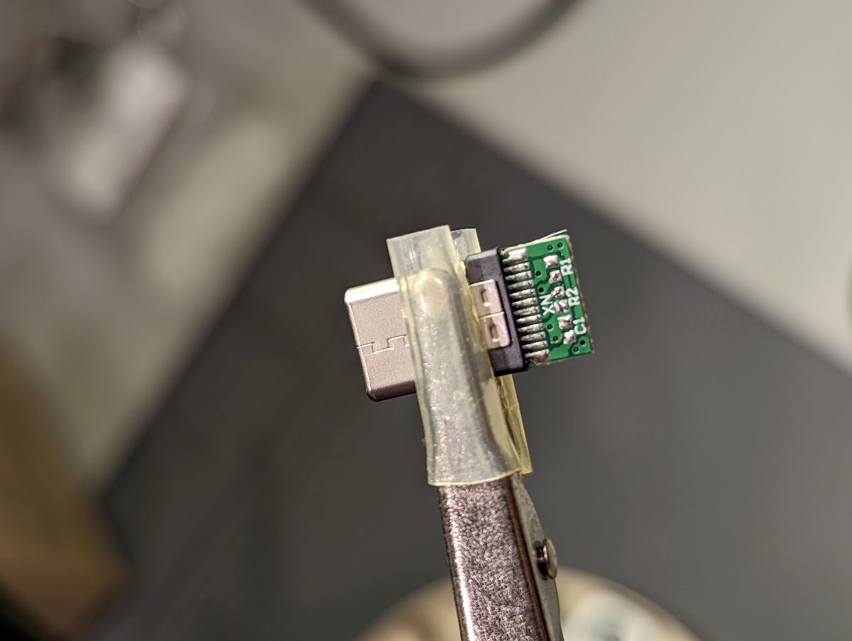
Right: The opposite side of the USB-C PCB has pins that are clearly labelled as G, D+, D-, and V. So we know to put the other lead of the pull-down resistor onto the big GND pad here. (This image was taken before I soldered the pull-down resistor onto the GND pad).
![]() FYI
FYI ![]() : If I was really precise, I would solder the resistor that was on R2, onto R1—this modification would be the cleanest way of configuring the USB-C connection to sub-device mode. But admittedly, I didn’t have this idea until after I completed the project.
: If I was really precise, I would solder the resistor that was on R2, onto R1—this modification would be the cleanest way of configuring the USB-C connection to sub-device mode. But admittedly, I didn’t have this idea until after I completed the project.
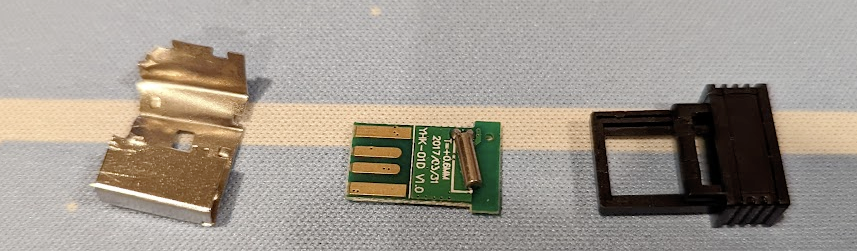
We’re done doing the most finicky soldering work! Now we just need to connect the G, D+, D-, and V pins to the Bluetooth module. To do this, we first need to open up the Bluetooth module. I use a pair of needle-nose pliers:
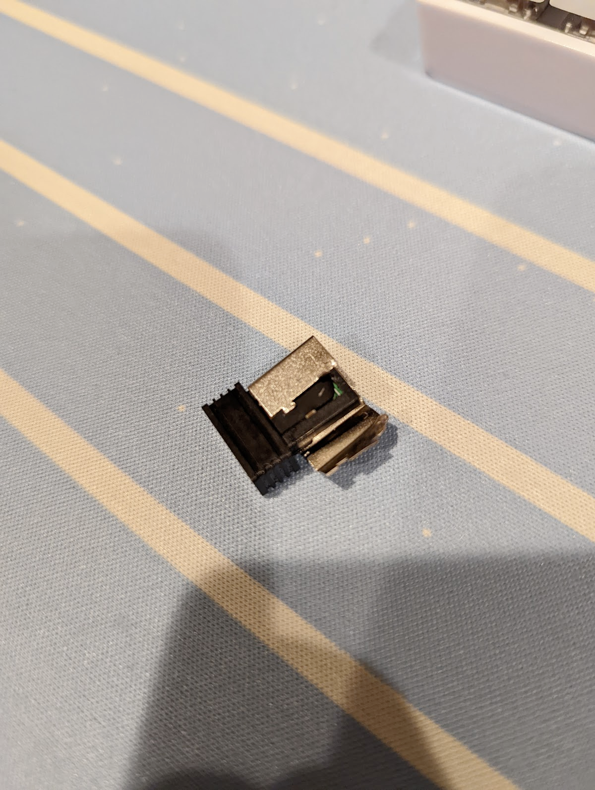
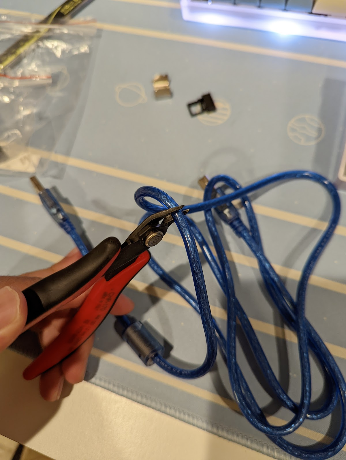
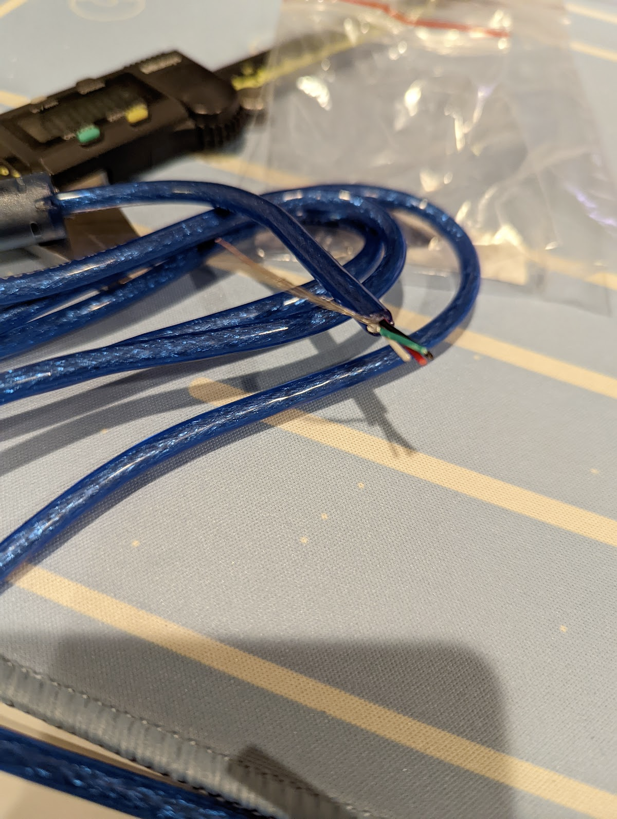
Next, we’re going to want some thin wires. Rather than purchase a bunch of such wires, the DIY Perks video cleverly suggests just stripping some old USB cable.
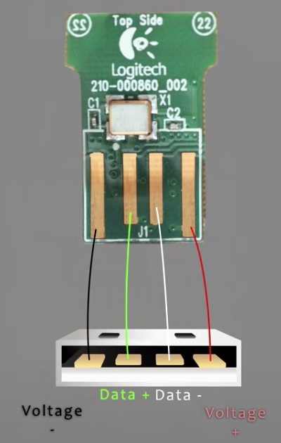
Now we just need to solder the wires together. Our USB-C breakout board has very clearly labelled pads, for GND, D+, D-, and V, so wiring those pads up is easy. The Bluetooth PCB that has the original USB-A port will, by definition, have its stereotypically shaped 4 pads in the following orientation:
Once we solder those wires together, we’re all done with the electronics!
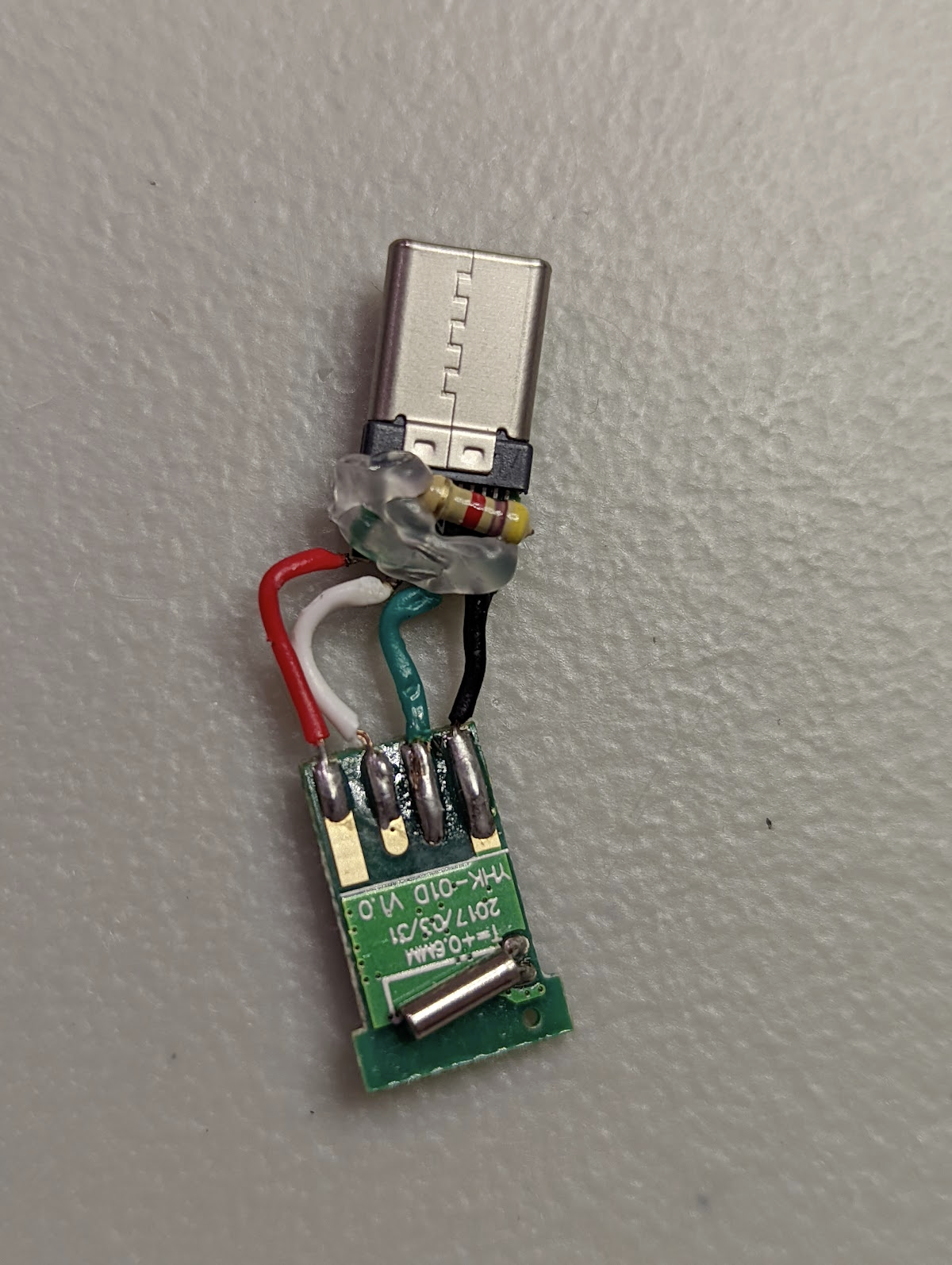
We then add some Sugru to cover up the bare electronics (or if you’d like, 2-part epoxy), and wait about 24 hours for the Sugru to dry!
Here’s a video of the operational USB-C receiver! I replaced the grey Sugru casing for a black one!